
I would argue that the single most important specification drafted by the ORAN Alliance is the fronthaul spec, O-RAN.WG4.CUS.0-v05.00, Control, User and Synchronization Plane Specification, published by the Fronthaul Working Group (WG4). This is the foundation of any eventual interoperability among radio and baseband OEMs, which is the holy grail of vendor diversity in the RAN.
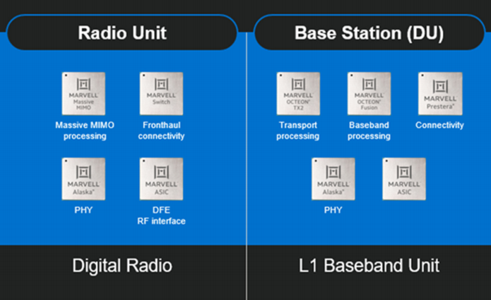
It’s well-known that WG4 settled on a 7.2 functional split between baseband (DU) and radio (RU), and this determines which functions are in which element. The key thing is that the PHY layer is split between the two, so high-PHY in the DU (along with the MAC layer) and low-PHY in the RU (along with DFE layer — Digital Front End signal processing).
The preferred fronthaul is of course eCPRI carried over any ethernet-compatible medium, generally fiber.
All of these functions are real-time compute-intensive. This is why the notion of a general-purpose Commercial Off The Shelf (COTS) server as a DU platform is a pipe dream. Any DU that supports more than a couple of microcells needs hardware acceleration that is unlikely to be found in a conventional datacenter server.
Early on, both Xilinx and Intel positioned themselves to provide this acceleration using their respective FPGA technologies. Intel even developed a ‘framework’ called FlexRAN based on a high-PHY binary hosted on x86. The acceleration comprises a look-aside Forward Error Correction accelerator and a pass-through eCPRI/fronthaul function, both implemented in an FPGA-based accelerator card. The x86 high-PHY has plenty to do, including scrambling, modulation, I/Q compression, and precoding for Category-A radios.
A no-cost high-PHY binary must seem attractive to new vRAN players, but it comes with a catch. It only works on certain Intel processors. Not AMD. Certainly not ARM. And this is most likely the point.
And there is another catch. The FlexRAN data path is convoluted, apparently running from the CU interface (F1 fiber connections) into memory, then out to the accelerator for FEC, then back into memory for the high-PHY, then out to the accelerator again for eCPRI and the fronthaul connectors. And the reverse for uplink. This looks unavoidable with the high-PHY anchored to the processor. And it looks inefficient.
Likewise, Intel and Xilinx both positioned themselves to provide real-time signal processing for the RU, Xilinx famously with its family of RFSoCs, and Intel by marrying its digital-only FPGAs with Analog Devices’ RFICs for DFE and AD/DA.
So . . . FPGAs in both RU and DU.
Now, for a given functionality, FPGAs are famously pricey as well as power-hungry. But this is supposed to be the price you pay for the ‘P’ in ‘Field Programmable Gate Array’. And with all the evolving standards (new 3GPP releases, incomplete fronthaul spec) and on-going research (beam-forming, precoding, etc., etc.) — not to mention undetected bugs — non-programmability is out of the question. Right? No one in their right mind would make a 6 to 7 figure investment in an ASIC to perform these functions, even if it did cut power and costs in half. ASICs can’t be changed, and you’d never recover your investment before having to replace it with an upgraded version. With an FPGA, you can always do a ‘firmware’ upgrade.
On the other hand . . .

This happy gentleman is showing off Ericsson’s latest generation of 64T64R 320W massive MIMO RU for band 77. Actually what he’s showing off is the weight — 20kG — achieved in no small part with a 20% further reduction in power consumption over the previous generation, with corresponding reduction in heat sinks and power supplies. And Ericsson is of course known for its performance-enhancing ‘Uplink Booster’ technology. Which makes for a formidable combination.
Ericsson is also well-known for using ASICs. How are they able? The Ericsson Many Core Architecture is to radio signal processing what a GPU is to image processing, or artificial intelligence. GPUs are programmable, and so is EMCA. It just happens to be purpose-built for DU and RU real-time compute-intensive work loads.
Of course, Ericsson does not sell EMCA silicon to the competition. One commercial alternative is Marvell’s newly-announced Octeon Fusion-O family, which can be programmed for high- and low-PHY, eCPRI, beam-forming, etc., and married with Analog Devices’ transceivers for at least some DFE functions plus AD/DA. They probably cut power consumption by half or better over FPGAs, and in the DU the high-PHY is hosted by the accelerator rather than the server’s processor, so the data path should be simpler — less churn through memory.
Another alternative (for the DU) is Nvidia’s Aerial SDK hosted on a GPU and providing PHY, FEC coding, beam-forming for Category-A RUs, and possibly eCPRI. This kind of solution is also very intriguing for the possibility of a common HW platform to support cloud RAN as well as AI work loads, which should be of interest in the edge network.
Xilinx knows they have an issue, and their newest generation of RFSoCs (due out later this year) introduces so-called hard blocks for DFE functions.
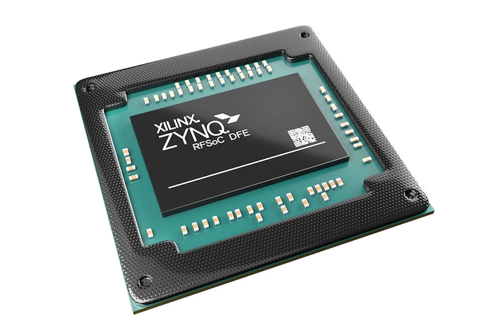
This is a step in the right direction, at least for the RU, although a major role will still be played by conventional programmable logic fabric.
All of these solutions to RU/DU signal processing are programmable. But they are not all FPGAs. It may be possible for the open RAN ecosystem to eventually rival Ericsson’s power efficiency (and hence KPIs like weight), without sacrificing flexibility. But they’ll have to escape the FPGA trap to do it.
